
In the world of printed circuit board (PCB) manufacturing, ensuring the highest levels of quality and reliability is non-negotiable. One of the most critical quality control steps in the production process is Automated Optical Inspection (AOI). AOI inspection and testing help manufacturers detect defects early, improve yields, and maintain consistent production standards.
What is AOI Inspection?
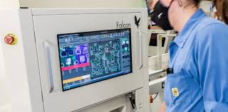
Automated Optical Inspection (AOI) is a non-contact visual inspection method used in the manufacturing of PCBs to detect a wide range of defects. AOI systems use high-resolution cameras, lighting systems, and advanced image-processing software to scan the surface of the board for anomalies.
The AOI machine compares the scanned image of the PCB to a pre-defined “golden board” reference. If any deviation is detected — such as missing components, incorrect orientation, soldering issues, or misaligned parts — the system flags the error for further review.
Why is AOI Important?
AOI plays a critical role in early defect detection, which minimizes costly rework and prevents defective boards from moving further down the production line. By catching issues during the assembly phase, manufacturers can save time, reduce waste, and deliver high-quality products to their clients.
Types of Defects Detected by AOI
AOI can identify a variety of issues in both pre-reflow and post-reflow inspection stages, including:
- Missing components
- Incorrect polarity or placement
- Tombstoning of passive components
- Solder bridges
- Insufficient or excess solder
- Misaligned ICs
- Open circuits
How Does AOI Work?
- Image Capture: The AOI system uses cameras to capture images of the board under inspection.
- Lighting Techniques: Different lighting methods (e.g., top-down, angled, or 3D) help reveal defects that might otherwise go unnoticed.
- Image Comparison: The captured image is compared against a reference image or design file.
- Defect Identification: Any mismatches or anomalies are flagged by the system.
- Operator Review: An operator may review flagged images for confirmation or further testing.
AOI vs. Other Inspection Methods
- Manual Inspection: Prone to human error, especially with complex PCBs.
- X-ray Inspection: Ideal for hidden solder joints (e.g., BGA), but more expensive and time-consuming.
- ICT (In-Circuit Testing): Good for electrical performance testing but requires custom fixtures.
- Functional Testing: Ensures the PCB works as intended but doesn’t detect physical defects like misalignments or poor soldering.
AOI complements these techniques and is especially valuable for detecting cosmetic and structural flaws.
Benefits of AOI Inspection
- High accuracy and repeatability
- Reduced labor cost and inspection time
- Early defect detection in the process
- Improved production yield
- Real-time feedback for process improvement
AOI in SMT and Through-Hole Assembly
While AOI is most commonly used in Surface Mount Technology (SMT) assembly, it is increasingly being adapted for through-hole component inspection as well. Modern AOI machines can handle a variety of board sizes, densities, and component types.
3D AOI – The Next Step
Advanced systems now offer 3D AOI, which uses structured light projection and multiple cameras to build a 3D model of the board surface. This technology enhances defect detection, especially for solder joint volume, height, and shape — critical for fine-pitch components and densely populated boards.
Conclusion
Automated Optical Inspection is an essential tool in modern PCB manufacturing. It enhances product reliability, reduces operational costs, and supports high-speed production lines with consistent inspection quality. Whether used as a standalone quality control step or in combination with other testing methods, AOI ensures that only defect-free PCBs make it to the next stage of your product lifecycle.