
How Cleanroom PPE Influences Semiconductor Yield Rates
In microelectronics manufacturing, even a single microscopic contaminant can lead to costly wafer defects. While fabs invest heavily in advanced lithography tools, air filtration systems, and process automation, one crucial variable often receives less attention: semiconductor cleanroom PPE.
Human-generated contamination remains one of the leading contributors to yield loss. The right cleanroom personal protective equipment plays a direct role in contamination control—and ultimately, in yield improvement.
The Relationship Between Contamination and Yield Loss
Semiconductor fabrication processes operate at nanometer-level precision. Particles invisible to the naked eye can cause:
- Pattern distortion during lithography
- Short circuits or open connections
- Defective dies on wafers
Even with high-grade HEPA and ULPA filtration, contamination introduced by personnel movement can compromise controlled environments. This is where effective contamination reduction strategies must extend beyond infrastructure and into operational discipline.
Why Semiconductor Cleanroom PPE Matters
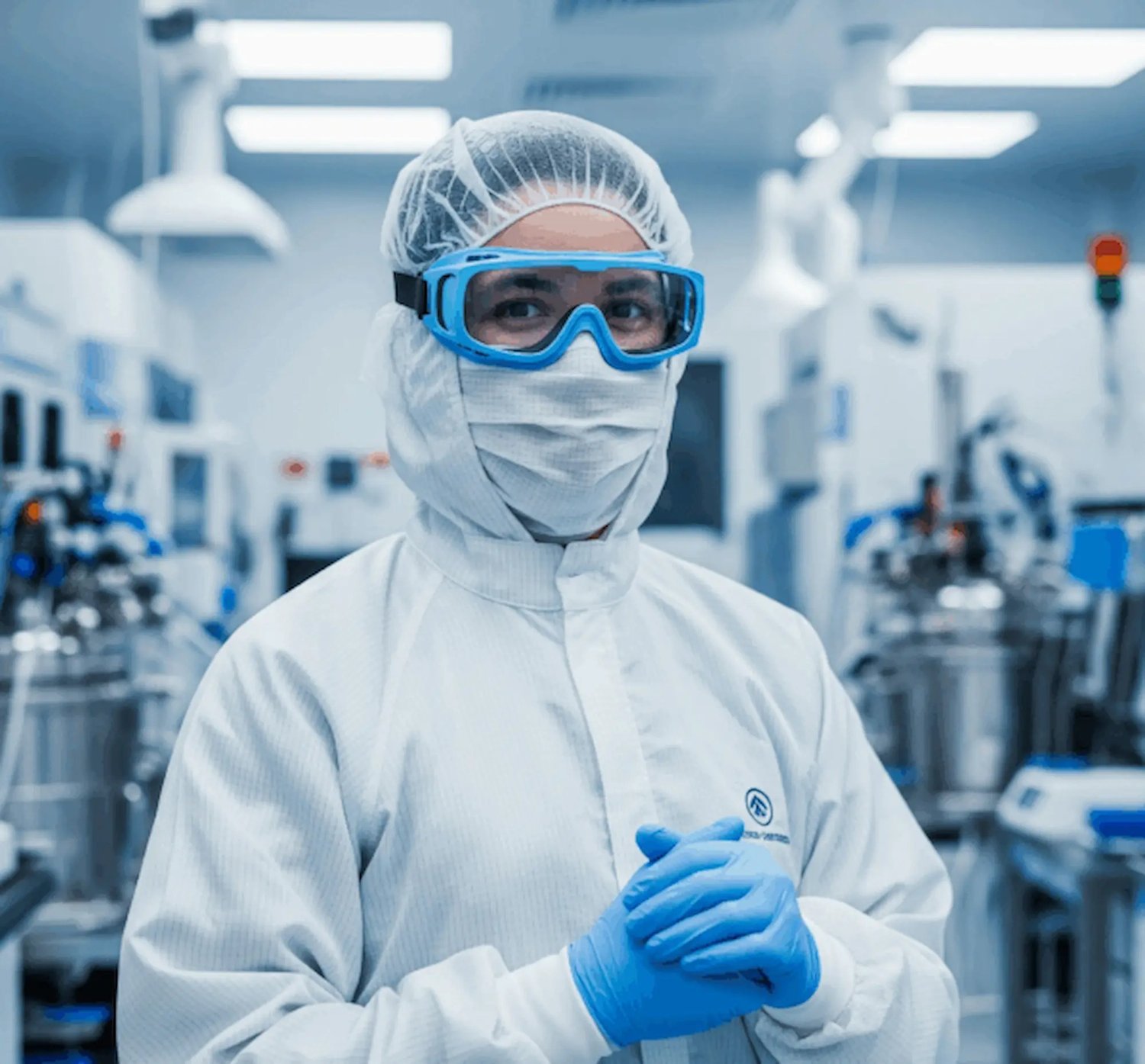
Personnel are one of the largest contamination sources in cleanrooms due to skin flakes, hair, fibers, and static-related particle attraction. Semiconductor cleanroom PPE is designed to minimize this risk by acting as a controlled barrier between the operator and the environment.
Key PPE elements include:
- Low-lint coveralls and gowns
- Antistatic gloves and footwear
- Face masks and hoods
- Eye protection compatible with cleanroom protocols
Each component is engineered to reduce particle shedding while supporting electrostatic discharge (ESD) control—critical in semiconductor fabs.
PPE’s Direct Impact on Yield Improvement
Properly selected and consistently used PPE contributes to measurable yield improvement by:
- Reducing random particle events on wafers
- Maintaining stable cleanroom classifications during operations
- Preventing cross-contamination between process zones
Over time, fabs that standardize PPE usage often report fewer process deviations and higher wafer acceptance rates.
Common PPE-Related Gaps in Semiconductor Fabs
Despite advanced tooling, many facilities still experience yield loss due to avoidable PPE issues, such as:
- Using generic cleanroom garments not suited for semiconductor environments
- Inconsistent gowning procedures across shifts
- Reusing disposable PPE beyond recommended cycles
- Lack of training on contamination-sensitive movements
These gaps highlight the importance of viewing PPE as part of the manufacturing process—not just a safety requirement.
Cleanroom PPE Selection for Microelectronics Manufacturing
Selecting the right protective equipment requires alignment with:
- Cleanroom class and process sensitivity
- ESD protection requirements
- Operator comfort to minimize unnecessary movement
- Material properties such as antistatic, low-lint, and breathable fabrics
Working with an experienced supplier like Klaritex ensures that PPE is purpose-built for semiconductor applications, supporting both contamination control and long-term operational efficiency.
Final Thoughts
Yield optimization in semiconductor manufacturing is not driven by equipment alone. It depends on a system where infrastructure, processes, and people work in harmony.
By prioritizing high-quality semiconductor cleanroom PPE, fabs can significantly reduce contamination risks, improve yield consistency, and protect their investment in advanced manufacturing technologies.