
DRAM operations are performed using a single capacitor and a single transistor, and their functionality completely depends on the charge stored in the capacitor. DRAM, a crucial component in computer memory systems, was invented by Robert Dennard in 1966 at IBM.
Working of DRAM
Dynamic Random Access Memory (DRAM) uses two elements as a storage cell like as transistor and capacitor. To keep charge or discharge of capacitors to be using the transistor.
If logic high or “1” it means capacitor has fully charging otherwise it gets discharge then its logic low or “0”. All operations of charging or discharging are performing by work line and bit line. Show in figure

DRAM Operations Are
There are two functions of DRAM; like as
- Write operation
- Reading Operation
Write Operation
In this operation, Voltage is going to supply on bit line as well as signal gets supply on the address line for closing the transistor in computer systems.
Reading Operation
While storing information in the cell, the transistor turns on and supplies voltage to the bit line. This process stores some charge in the capacitor. After a short period, the transistor switches off, and the capacitor gradually discharges. As a result, all the information is stored in the cell, which can be read easily. In modern multi-core computer systems, efficient DRAM operation is essential to ensure fast and synchronized data access across all cores.
There are various lines which are using in the Read and Write Operations; such as –
- /CAS, the Column Address Strobe: This line helps to choose the column to be addressing. Address inputs get obtaining on the falling edge of/CAS. It gets to enable a column that chosen from the open row for getting read or write operations.
- /OE, Output Enable: The /OE gets to use, if controlling several memory chips in parallel form. It helps to handle the output to data I/O pins. If /RAS and /CAS get to low, /WE is high, and /OE is also getting low, then data pins driven by DRAM chip.
- /RAS, the Row Address Strobe: The /RAS line selects the row to be address. Address inputs get obtain on the falling edges of the /RAS line. The row is getting to open as long as /RAS remains low.
- /WE, Write Enable: The signal monitors that falling edge of /CAS is read or writes. High enables a read action but low enables the write action. Data inputs also captured on the falling edge of /CAS.
How to Organize DRAM?
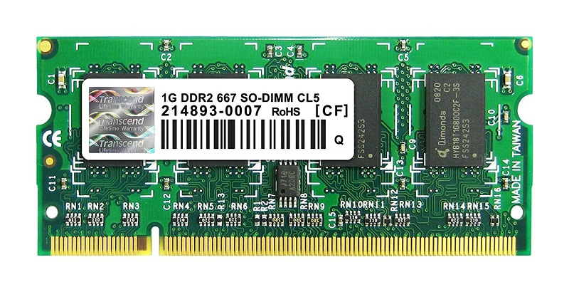
Today’s, Dynamic RAM is available in different types of forms but it depends upon their applications; for example – DIMM (Dual Inline Memory Module) consists several onboard DRAM chips.
These types of DIMMs have 1 GB memory, but you can see “2Rx8” written on the sticker. 2R represents that this module comes in rank 2, but x8 mean and that output width of data coming from every DRAM chips.

A rank is a individual addressable group of DRAMs. In this scenario, one rank is group of four DRAM chips, but we have 2 ranks if there are 8 total.
DIMM has higher level of organization with getting of DRAM’s rank. Mention in the figure that, every chip organizes into number of memory arrays and banks, and columns. Show in the image, DRAM chip has four banks.
Each bank works individually to the others, it means all operations such as reading, writing, and pre-recharging can perform on bank without stressing to other.